大声
【扒一扒】日本高纯球形硅微粉材料生产商
—— anndi

《【扒一扒】日本高纯球形硅微粉材料生产商》:  作为一种无机非金属矿物功能性粉体材料,硅微粉广泛应用于电子材料、电工绝缘材料、胶黏剂、特种陶瓷、精密铸造、油漆涂料、油墨、硅橡胶等领域。 目前,世界上只有中国、日本、韩国、美国等少数国家具备硅微粉生产能力... 全文 ?

1

关于脱肟型硅胶对PC材料的影响

最近和一位网友讨论PC管套接时使用硅胶进行密封,PC管出现了裂纹和凹槽的情况,大致探讨如下,其实我也是现学现卖和他一起讨论的,自己也算是增加了一个知识点:

网友: Anndi,不知道您有沒有遇到過這樣的問題:PC管塗了密封膠固化之後出現管體的裂痕和凹槽。此密封膠固化過程中會產生酮胺基。而裂解的產物為一氧化矽、一氧化碳和微量的燃燒不完全的碳化物、氧化金屬和甲醛。我能得到的信息就這些,不知道您對此有什麼看法,麻煩您了。

anndi : 密封胶缩合型的会产生小分子物质(如醇类、酸类或酮类小分子物质),可能会对材料有腐蚀!但你说的裂解我个人觉得不大可能出现, 这个应该是常温固化的密封胶吧! 即使是加热固化应该也不会发生裂解的现象

网友: 這種密封膠屬於常溫固化類型,在與空氣接觸之後會產生醇類物質,但是PC管與密封膠接觸的部位沒有發現任何腐蝕現象,而是剩餘的管體發生變形而形成凹槽。個人認為是不是pc的內應力所引起的呢?

anndi : 不打胶没这个现象吗?

网友: 嗯嗯,是的,固話之後才有這個問題,估計是膠和pc發生某種反應而產生的

anndi : 如果是有机硅胶不应该会有这么大应力的,应该还是你所说的反应产物导致的,用的什么牌号的硅胶?

网友: 我們是台灣***的品牌,我這邊沒有msds

anndi : 哦,你可以自己做个实验试试

网友: 具體怎樣操作呢?

anndi : 如果是你说的现象那就基本可以可肯定是胶的问题,换别的密封胶试试

网友: 我們做過類似的實驗。採用不同品牌的矽膠對pc護欄管進行實驗,都發生了變形;之後,我們採用同一品牌密封膠,換不同品牌的pc管(德國拜耳生產和國內生產),但還是出現了一樣的問題。不過今天發生了一件事情,我們用另外一種膠水,卻發現pc管沒有發生變形

anndi : 另外一种胶水不是有机硅系列吧

网友: 還是有机硅

anndi : 哦,有机硅分脱酸、脱醇、脱酮、脱甲醛等等

网友: 是的

anndi : 你们发生腐蚀的是脱什么的啊?

网友: 脱酮
anndi : 哦,那不腐蚀的呢
网友: 會釋放酮肟基,不腐蝕的是脱醇

anndi : 脱酮肟型的不适用于PC的密封,对铜也有腐蚀的

网友: 明白

anndi : 改用脱醇的好些

网友: 怪不得

anndi :
:)

再次复习一下知识点:

单组分室温硫化硅橡胶的硫化反应是靠空气中的水分来引发的。常用的交链剂是甲基三乙酰氧基硅烷,它的Si-O-C键很易被水解,乙酰氧基与水中的氢基结合成醋酸,而将水中的羟基移至原来的乙酰氧基的位置上,成为三羟基甲基硅烷。三羟基甲基硅烷极不稳定,易与端基为羟基的线型有机硅缩合而成为交链结构。平时,将含有硅醇端基的有机硅生胶与填料、催化剂、交链剂等各种配合剂装入密封的软管中,使用时由容器挤出,借助于空气中的水分而硫化成弹性体, 同时放出低分子物。交链剂除甲基三乙酰氧基硅烷外,还可以是含烷氧基、肟基、胺基、酰胺基、酮基的硅烷。当与烷氧基交链后放出醇,称为脱醇型单组分室温硫化硅橡胶,当与肟基交链后生成肟,称为脱肟型室温硫化硅橡胶、因此,随着交链剂的不同,单组分室温硫化硅橡胶可为脱酸型、脱肟型、脱醇型、脱胺型、脱酰胺型和脱酮型等许多品种。

0

Bonding, Sealing and Coating Solutions for Mobile Devices

在网上到处找3541和3542的TDS资料没找到,找到了一份汉高手机组装用胶点彩页,里面也提到了3541和3542,觉得不错,大家可以参考学习一下:

Henkel offers complete engineering services for projects demanding expertise and support beyond the limits of our standard technical services.
As a result, our engineers provide the following value-added services.
• On-site engineering assistance and consultation
• Joint product development programs
• Contract lab services and testing
• Prototype testing
• Custom formulations

Global Capabilities
We are the global technology leader with extensive network to support customers’ value chain.

Design Partnership
Our large experienced team of engineers provide documented design and application support.

Best-in-Class Technical Support
Our professional engineering support empowers our customers to improve their quality and efficiency.

Innovative & Sustainable Solutions
We enable customers’ innovation to meet fast design changes and development with green solutions.

Cost Saving & Reliability
Our superior adhesives and equipment improve productivity, durability and reduce overall cost.

华为网盘下载:http://dl.dbank.com/c0gauebiaa

点击附件下载查看:

  Bonding_Sealing_and_Coating_Solutions_for_Mobile_Devices (1.3 MB, 19 次)
您没有权限下载此文件。

2

乐泰柔性瞬干胶410 TDS

产品说明
LOCTITE® 410™ 具有下列性能
技术氰基丙烯酸酯
化学类型氰基丙烯酸乙酯
外观(未固化) 黑色液体LMS
组成单组分-无需混合
粘度高
固化方式湿汽固化
应用粘接
主要粘接基材金属, 塑料和橡胶
LOCTITE® 410™ 是橡胶增强型瞬干胶,提高了柔韧性和剥
离强度,增加了抗振动的性能.
固化前的材料特性
比重@ 25 °C 1,1
粘度, Brookfield – RVT, 25 °C, mPa·s (cP):
转子 3, 转速20 rpm 1 700-5 000LMS
闪点 – 见MSDS
典型固化特性一般情况下,材料表面的湿气会引发本产品
的固化反应。尽管本产品在相当短的时间内就可达到完全
实用强度,但是至少要继续固化24小时才能具有完全的耐
化学/溶剂性能。
固化速度与基材的关系
固化速度取决于被粘界的基材,下表表明在22 °C / 50
% 相对湿度的情况下,不同基材的固定时间。试样的剪
切强度达到0.1 N/mm². 所需要的时间。
固定时间, 秒:
钢材 (去脂) 60-120
铝10-30
氯丁橡胶15-25
丁腈橡胶15-25
ABS 20-50
PVC 50-100
聚碳酸酯30-90
酚醛树脂20-60
固化速度与间隙的关系
固化速率取决于粘接间隙。粘接间隙小固化速度快,粘接
间隙增大将降低固化速度.
固化速度与促进剂的关系
粘接间隙过大,致使固化太慢时,在基材表面使用促进剂
可以提高固化速度。但是这样处理会降低粘接的最终强度
。因此建议进行试验以确定实际可达到的性能.

固化后材料典型性能
后24小时 @ 22 °C
物理性能:
热膨胀系数 ISO 11359-2, K-1 80×10-6
导热系数, ISO 8302, W/(m·K) 0,1
玻璃转化温度, ASTM E 228, °C 120
电性能:
介电常数/损失, IEC 60250:
0,05-kHz 2,3 / <0,02
1-kHz 2,3 / <0,02
1 000-kHz 2,3 / <0,02
体积电阻率, IEC 60093, ·cm 10×1015
介电强度, IEC 60243-1, kV/mm 25
固化后材料特性
胶粘剂性能
24小时后 @ 22 °C
剪切强度, ISO 4587:
钢材(喷砂) N/mm² 22
(psi) (3 190)
铝 (蚀刻) N/mm² 15
(psi) (2 175)
ABS N/mm² >6
(psi) (>870)
PVC N/mm² >6
(psi) (>870)
聚碳酸酯 N/mm² >5
(psi) (>725)
酚醛树脂 N/mm² 10
(psi) (1 450)
氯丁橡胶 N/mm² >10
(psi) (>1 450)
丁腈橡胶 N/mm² >10
(psi) (>1 450)
抗拉强度, ISO 6922:
钢材(喷砂) N/mm² 18,5
(psi) (2 680)
后48小时 @ 22 °C
剪切强度, ISO 4587:
钢材(喷砂) N/mm² ≥15,8
(psi) (≥2 290)
65 °C时固化12小时, 之后@ 22 °C进行4小时固化
剪切强度, ISO 4587:
钢材(喷砂) N/mm² ≥19,3LMS
(psi) (≥2 800)

典型环境抵抗性能
1周后 @ 22 °C
剪切强度, ISO 4587:
低碳钢(喷砂)
热强度
在测试温度下进行强度测试
% 强度
温度(°C)
100
75
50
25
0
0 60 80 100 120
老化强度
在测试温度下进行老化,在22 °C进行测试
% 初始强度
时间
150
125
100
75
50
25
0
24 100 500 1000 5000
80 °C
100 °C
耐化学品/溶剂测试
在下列条件下进行老化,在22 °C进行测试.
初始粘结强度的剩有率%
环境°C 100 h 500 h 1000 h
机油(MIL-L-46152) 40 85 85 85
汽油22 90 70 70
异丙醇22 75 75 75
工业甲基化酒精22 95 95 80
1,1,1 三氯乙烷22 80 70 50
氟立昂 TA 22 90 90 85
热/湿95% RH 40 100 100 100
注意事项
本产品不宜在纯氧与(或)富氧环境中使用,不能作为氯
气或其它强氧化性物质的密封材料使用。
有关本产品的安全注意事项,请查阅乐泰的材料安全数据
资料(MSDS).

使用指南
1. 要想获得最好的粘接性能,被粘接的材料表面应当干
净,无油脂.
2. 本产品最适合较小间隙 (0.05 mm)的粘接.
3. 多余的胶粘剂可用乐泰清洗剂,硝基甲烷或丙酮溶解
.
乐泰材料说明LMS
LMS于6月-13, 2001. 每一批号产品都有测试报告
。LMS测试报告中含有一些对客户有用的质检测试参数
。此外,我们也通过多种质量控制,确保产品质量的一致
性。特殊客户的要求可以由汉高乐泰质量中心负责协调。
贮存条件
产品贮存于未开封的原包装内存放在阴凉干燥处。贮存方
法在产品外包装上有所标注。
理想贮存条件: 2 °C to 8 °C. 如将该产品贮存在低
于2 °C或高于8 °C 的温度条件下,可能会影响产品性
能.
被取出包装盒外使用的产品有可能在使用中受到污染。为
避免污染未用胶液,不要将任何胶液倒回原包装内。本公
司将不会对已受到污染的或上面已提及的贮存方法不恰当
的产品负责。如需更多信息,请与当地的乐泰公司技术服
务部或客户服务部联系。
单位换算
(°C x 1.8) + 32 = °F
kV/mm x 25.4 = V/mil
mm / 25.4 = inches
μm / 25.4 = mil
N x 0.225 = lb
N/mm x 5.71 = lb/in
N/mm² x 145 = psi
MPa x 145 = psi
N·m x 8.851 = lb·in
N·m x 0.738 = lb·ft
N·mm x 0.142 = oz·in
mPa·s = cP
说明
本文中所含的各种数据仅供参考,并被认为是可靠的。对
于任何人采用我们无法控制的方法得到的结果,我们恕不
负责。自行决定把本产品用在本文中提及的生产方法上
,及采取本文中提及的措施来防止产品在贮存和使用过程
中可能发生的损失和人身伤害都是用户自己的责任。鉴于
汉高乐泰公司明确声明对所有因销售乐泰产品或特定场合
下使用乐泰产品而出现的所有问题,包括针对某一特殊用
途的可商品化和适用性的问题,不承担责任。汉高乐泰公
司明确声明对任何必然的或意外损失包括利润方面的损失
都不承担责任。本文中所论述的各种生产工艺或化学成分
都不能被理解为这些专利可以被其他人随便使用和拥有或
被理解为得到了包括这些生产工艺和化学成分的汉高公司
的专利许可证。建议用户每次在正式使用前都要根据本文
提供的数据先做实验。本产品受美国、外国专利或专利应
用的保护。


下载附件查看PDF文件:

  loctite 410 TDS (91.0 KB, 8 次)
您没有权限下载此文件。

1

日本施敏打硬Cemedine环氧粘接剂EP138

最近一个客户在评估一款耐高温的电机胶水,他们日本客户推荐了这款产品,我在网上查看了一下,属于单组分热固化环氧胶粘剂,而且此产品似乎也用于喇叭粘接等其他用途。他们的官网上列举了不少型号,EP138也是其中一种,但是似乎没有能找到其tds资料,倒是从一个朋友那里拿到了一份MSDS资料。放在文章末尾大家可以下载查看!其官网提供的资料如下:
Epoxy resin adhesive refers to the adhesive which cures chemicals containing epoxy group with amines and acid anhydride.

Features

  1. Reactive adhesive
  2. Solventless
  3. No gas produced during curing process
  4. Excellent adhesive strength
  5. Excellent heat and chemicals resistance
  6. Small shrinkage by curing
  7. Small creep under load
  8. Excellent durability
  9. Superb insulation

Application

Applicable to adherents over an extensive range including metals and plastics

• Adhesion of cars, vehicles, vessels and aircraft • Adhesion and sealing of electric equipment and electronic parts
• Adhesion of composite members for construction • Assembly of precision equipment and art works
• Adhesion of sporting equipment


Adhesive strength for various types of materials

Tensile shear strength (unit: N/mm2)
Product name 1500 EP007 EP330
Adherend
Iron 15.5 15.0 17.6
Aluminum 6.0 13.0 10.2
Stainless steel 22.0 16.3
Copper 7.8 10.0 19.8
Unplasticized polyvinyl chloride 3.5 4.1*
Styrene resin 1.9 1.9 0.9
Acrylic resin 2.9 1.0 0.9
FRP 12.3 8.0 3.9
Melamine facing plate 5.4 43.1
Lauan plywood 10.4* 10.0* 47.1*

An asterisk (*) indicates material failure.

Chemical resistance test

Tensile shear strength (unit: N/mm2)
Product name 1500 EP007 EP138
Chemicals
Blank 14.0 20.1 29.4
Acetone 12.5 17.6
Toluene 12.5 17.3 32.2
Trichloroethylene 12.8 17.4 31.1
Methanol 12.0 17.4 30.6
Gasoline 13.6 19.4 31.3
Engine oil 11.2 21.5 31.2
10% sulfuric acid 10.5 19.3 22.8
10% NaOH 13.6 20.4 25.3
Tap water 13.1 21.5 28.4


Dependency adhesive strength on temperature

Two-part adhesive to be cured at normal temperature adhesives (general purpose)

Two-part adhesive to be cured at normal temperature adhesives

One-part thermosetting epoxy resin adhesive

可以到这个链接查看:http://www.cemedine.co.jp/e/product/epoxy.html

 
点击下载附件查看:

  cemedine ep138 tds (643.7 KB, 10 次)
您没有权限下载此文件。

1

Ablestik 导电银胶2030SC TDS

PRODUCT DESCRIPTION
ABLEBOND 2030SC provides the following product
characteristics:
Technology Proprietary Hybrid Chemistry
Appearance Silver
Cure Heat cure
pH 4.5
Product Benefits • Snap curable
• Low stress
Application Die attach
Filler Type Silver
Key Substrates Most metals
ABLEBOND 2030SC die attach adhesive has been formulated
for use in high throughput die attach applications. This material
is designed to minimize stress and resulting warpage between
dissimilar surfaces. It can be used in a variety of package sizes
.
TYPICAL PROPERTIES OF UNCURED MATERIAL
Thixotropic Index (0.5/5 rpm) 4.6
Viscosity, Brookfield CP51, 25 °C, mPa·s (cP):
Speed 5 rpm 11,600
Work Life @ 25°C, hours 24
Shelf Life @ -40°C (from date of manufacture), year 1
TYPICAL CURING PERFORMANCE
Cure Schedule
90 seconds @ 110°C
Alternative Cure Schedule
10 seconds @ 150°C
Weight Loss on Cure
10 x 10 mm Si die on glass slide, % 0.4
The above cure profiles are guideline recommendations. Cure
conditions (time and temperature) may vary based on customers'
experience and their application requirements, as well as customer
curing equipment, oven loading and actual oven temperatures.
TYPICAL PROPERTIES OF CURED MATERIAL
Physical Properties:
Thermal Conductivity, W/mK 2.3
Tensile Modulus, DMTA :
@ -65 °C N/mm² 6,200
(psi) (900,000)
@ 25 °C N/mm² 3,300
(psi) (480,000)
@ 150 °C N/mm² 350
(psi) (50,000)
@ 250 °C N/mm² 450
(psi) (65,000)
Extractable Ionic Content, @ 100°C ppm:
Chloride (Cl-) <20
Sodium (Na+) <30
Potassium (K+) <5
Weight Loss After Cure, %:
16 hours Isothermal @ 125ºC 0.41
Ramp to 230ºC 0.5
Electrical Properties:
Volume Resistivity, ohms-cm:
cured 90 seconds @ 110ºC 0.0002
Bond Joint Resistance, ohms:
cured 90 seconds @ 110ºC, Cu/Cu, 25μm Bondline 0.008
TYPICAL PERFORMANCE OF CURED MATERIAL
Die Shear Strength vs Substrate:
2 X 2 mm die, kg-f,
Die on Substrate: @ RT
Si die on Pd 1.90
Au die on SS 2.24
Au die on Au 2.11
Die Shear Strength vs Die Shear Temperature:
3 X 3 mm Si die, kg-f,
cured 90 seconds @ 110ºC
Substrate @25°C @150°C @200°C
PBGA-FR4 1.90 0.96 0.87
GENERAL INFORMATION
For safe handling information on this product, consult the
Material Safety Data Sheet, (MSDS).
THAWING:
1. Allow container to reach room temperature before use.
2. After removing from the freezer, set the syringes to stand
vertically while thawing.
3. Refer to the Syringe Thaw time chart for the thaw time
recommendation.
4. DO NOT open the container before contents reach 25°C
temperature. Any moisture that collects on the thawed
container should be removed prior to opening the
container.
5. DO NOT re-freeze. Once thawed to -40°C, the adhesive
should not be re-frozen.
Temperature, °C
Syringe Thaw Time, Minutes
30
20
10
0
-10
-20
-30
-40
0 10 20 30 40 50
1cc
3cc 10cc 30cc
DIRECTIONS FOR USE
1. Thawed adhesive should be immediately placed on
dispense equipment for use.
2. If the adhesive is transferred to a final dispensing
reservoir, care must be exercised to avoid entrapment of
contaminants and/or air into the adhesive.
3. Adhesive must be completely used within the products
recommended work life of 24 hours.
4. Silver-resin separation may occur if the adhesive is left
out at 25°C beyond the recommended work life.
Not for product specifications
The technical data contained herein are intended as reference
only. Please contact your local quality department for
assistance and recommendations on specifications for this
product.
Storage
Store product in the unopened container in a dry location.
Storage information may be indicated on the product container
labeling.
Optimal Storage: -40 °C. Storage below minus (-)40 °C or
greater than minus (-)40 °C can adversely affect product
properties.
Material removed from containers may be contaminated during
use. Do not return product to the original container. Henkel
Corporation cannot assume responsibility for product which
has been contaminated or stored under conditions other than
those previously indicated. If additional information is required,
please contact your local Technical Service Center or
Customer Service Representative.
Conversions
(°C x 1.8) + 32 = °F
kV/mm x 25.4 = V/mil
mm / 25.4 = inches
N x 0.225 = lb
N/mm x 5.71 = lb/in
N/mm² x 145 = psi
MPa x 145 = psi
N·m x 8.851 = lb·in
N·m x 0.738 = lb·ft
N·mm x 0.142 = oz·in
mPa·s = cP
Note
The data contained herein are furnished for information only
and are believed to be reliable. We cannot assume
responsibility for the results obtained by others over whose
methods we have no control. It is the user's responsibility to
determine suitability for the user's purpose of any production
methods mentioned herein and to adopt such precautions as
may be advisable for the protection of property and of persons
against any hazards that may be involved in the handling and
use thereof. In light of the foregoing, Henkel Corporation
specifically disclaims all warranties expressed or implied,
including warranties of merchantability or fitness for a
particular purpose, arising from sale or use of Henkel
Corporation’s products. Henkel Corporation specifically
disclaims any liability for consequential or incidental
damages of any kind, including lost profits. The discussion
herein of various processes or compositions is not to be
interpreted as representation that they are free from
domination of patents owned by others or as a license under
any Henkel Corporation patents that may cover such
processes or compositions. We recommend that each
prospective user test his proposed application before repetitive
use, using this data as a guide. This product may be covered
by one or more United States or foreign patents or patent
applications.
下载附件查看PDF文件:

  ABLEBOND 2030SC-EN (65.4 KB, 13 次)
您没有权限下载此文件。

0

乐泰Cornerfill 3508 TDS

PRODUCT DESCRIPTION
3508™ provides the following product characteristics:
Technology Epoxy
Appearance Black
Components One component
Product Benefits • Reworkable
• Pb-free applications
• Eliminates post-reflow dispenses
and cure steps
• Improves mechanical reliability of
hand-held devices
Cure Reflow
Application Cornerfill
Typical Assembly
Applications
Chip scale packages and BGA
3508™ reworkable cornerfill is designed to cure during pb-free
reflow while allowing self-alignment of IC components. It can
be pre-applied to the board at the corners of the pad site
using a standard SMA dispenser.
TYPICAL PROPERTIES OF UNCURED MATERIAL
Viscosity, Cone & Plate,@ 25 °C mPa∙s (cP) 50,000
Specific Gravity @ 25 °C 1.24
Pot Life @ 25ºC, days >30
Shelf Life @ 2 to 8°C, months 6
Flash Point - See MSDS
TYPICAL CURING PERFORMANCE
Recommended Cure Schedule
Pb-free solder reflow profile @ 245°C
(3 hours @ 180°C for Tg testing)
The above cure profile is a guideline recommendation. Cure
conditions (time and temperature) may vary based on
customers' experience and their application requirements, as
well as customer curing equipment, oven loading and actual
oven temperatures.
TYPICAL PROPERTIES OF CURED MATERIAL
Physical Properties:
Coefficient of Thermal Expansion , ppm/°C:
Below Tg 55
Above Tg 175
Glass Transition Temperature (Tg) by TMA, °C 115
Shore Hardness, Durometer D 71
Storage Modulus, 25°C, GPa 2.48
Tensile Modulus N/mm² 1,130
(psi) (163,892)
Tensile Strength N/mm² 56.5
(psi) (8,190)
GENERAL INFORMATION
For safe handling information on this product, consult the
Material Safety Data Sheet, (MSDS).
This product is not recommended for use in pure oxygen
and/or oxygen rich systems and should not be selected as
a sealant for chlorine or other strong oxidizing materials.
Not for product specifications
The technical data contained herein are intended as reference
only. Please contact your local quality department for
assistance and recommendations on specifications for this
product.
Storage
Store product in the unopened container in a dry location.
Storage information may be indicated on the product container
labeling.
Optimal Storage: 2 to 8°C. Storage below 2°C or greater
than 8°C can adversely affect product properties.
Material removed from containers may be contaminated during
use. Do not return product to the original container. Henkel
Corporation cannot assume responsibility for product which
has been contaminated or stored under conditions other than
those previously indicated. If additional information is required,
please contact your local Technical Service Center or
Customer Service Representative.
Do not return products to refrigerated storage; any surplus
product should be discarded.
Conversions
(°C x 1.8) + 32 = °F
kV/mm x 25.4 = V/mil
mm / 25.4 = inches
N x 0.225 = lb
N/mm x 5.71 = lb/in
N/mm² x 145 = psi
MPa x 145 = psi
N·m x 8.851 = lb·in
N·m x 0.738 = lb·ft
N·mm x 0.142 = oz·in
mPa·s = cP
Note
The data contained herein are furnished for information only
and are believed to be reliable. We cannot assume
responsibility for the results obtained by others over whose
methods we have no control. It is the user's responsibility to
determine suitability for the user's purpose of any production
methods mentioned herein and to adopt such precautions as
may be advisable for the protection of property and of persons
against any hazards that may be involved in the handling and
use thereof. In light of the foregoing, Henkel Corporation
specifically disclaims all warranties expressed or implied,
including warranties of merchantability or fitness for a
particular purpose, arising from sale or use of Henkel
Corporation’s products. Henkel Corporation specifically
disclaims any liability for consequential or incidental
damages of any kind, including lost profits. The discussion
herein of various processes or compositions is not to be
interpreted as representation that they are free from
domination of patents owned by others or as a license under
any Henkel Corporation patents that may cover such
processes or compositions. We recommend that each
prospective user test his proposed application before repetitive
use, using this data as a guide. This product may be covered
by one or more United States or foreign patents or patent
applications.
下载附件查看PDF版本:

  loctite 3508 TDS (55.9 KB, 8 次)
您没有权限下载此文件。

0

Ablestik导电银胶ABLEBOND 8380B TDS

PRODUCT DESCRIPTION
ABLEBOND 8380B provides the following product
characteristics:
Technology Epoxy
Appearance Silver
Cure Heat cure
Product Benefits • Electrically conductive
• Fast cure at low temperatures
• Low resin bleed
Application Die attach
Filler Type Silver
Typical Package
Application
Charge Couple Device (CCD)
ABLEBOND 8380B adhesive is designed for medium die
attach applications.
TYPICAL PROPERTIES OF UNCURED MATERIAL
Thixotropic Index (0.5/5 rpm) 2.0
Viscosity, Brookfield CP51, 25 °C, mPa·s (cP):
Speed 5 rpm 10,000
Work Life @ 25°C, hours 48
Shelf Life @ -40°C (from date of manufacture), year 1
TYPICAL CURING PERFORMANCE
Cure Schedule
15 minutes @ 150°C
The above cure profiles are guideline recommendations. Cure
conditions (time and temperature) may vary based on customers'
experience and their application requirements, as well as customer
curing equipment, oven loading and actual oven temperatures.
TYPICAL PROPERTIES OF CURED MATERIAL
Electrical Properties:
Volume Resistivity, ohms-cm 0.0002
TYPICAL PERFORMANCE OF CURED MATERIAL
Die Shear Strength:
2 X 2 mm , psi,
cured 15 minutes @ 150ºC
Substrate
Ag/Cu Leadframe 1400
GENERAL INFORMATION
For safe handling information on this product, consult the
Material Safety Data Sheet, (MSDS).
THAWING:
1. Allow container to reach room temperature before use.
2. After removing from the freezer, set the syringes to stand
vertically while thawing.
3. Refer to the Syringe Thaw time chart for the thaw time
recommendation.
4. DO NOT open the container before contents reach 25°C
temperature. Any moisture that collects on the thawed
container should be removed prior to opening the
container.
5. DO NOT re-freeze. Once thawed to -40°C, the adhesive
should not be re-frozen.
Temperature, °C
Syringe Thaw Time, Minutes
30
20
10
0
-10
-20
-30
-40
0 10 20 30 40 50
1cc
3cc 10cc 30cc
DIRECTIONS FOR USE
1. Thawed adhesive should be immediately placed on
dispense equipment for use.
2. If the adhesive is transferred to a final dispensing
reservoir, care must be exercised to avoid entrapment of
contaminants and/or air into the adhesive.
3. Adhesive must be completely used within the products
recommended work life of 24 hours.
4. Silver-resin separation may occur if the adhesive is left
out at 25°C beyond the recommended work life.
Not for product specifications
The technical data contained herein are intended as reference
only. Please contact your local quality department for
assistance and recommendations on specifications for this
product.
Storage
Store product in the unopened container in a dry location.
Storage information may be indicated on the product container
labeling.
Optimal Storage: -40 °C. Storage below minus (-)40 °C or
greater than minus (-)40 °C can adversely affect product
properties.
Material removed from containers may be contaminated during
use. Do not return product to the original container. Henkel
Corporation cannot assume responsibility for product which
has been contaminated or stored under conditions other than
those previously indicated. If additional information is required,
please contact your local Technical Service Center or
Customer Service Representative.
Conversions
(°C x 1.8) + 32 = °F
kV/mm x 25.4 = V/mil
mm / 25.4 = inches
N x 0.225 = lb
N/mm x 5.71 = lb/in
N/mm² x 145 = psi
MPa x 145 = psi
N·m x 8.851 = lb·in
N·m x 0.738 = lb·ft
N·mm x 0.142 = oz·in
mPa·s = cP
Note
The data contained herein are furnished for information only
and are believed to be reliable. We cannot assume
responsibility for the results obtained by others over whose
methods we have no control. It is the user's responsibility to
determine suitability for the user's purpose of any production
methods mentioned herein and to adopt such precautions as
may be advisable for the protection of property and of persons
against any hazards that may be involved in the handling and
use thereof. In light of the foregoing, Henkel Corporation
specifically disclaims all warranties expressed or implied,
including warranties of merchantability or fitness for a
particular purpose, arising from sale or use of Henkel
Corporation’s products. Henkel Corporation specifically
disclaims any liability for consequential or incidental
damages of any kind, including lost profits. The discussion
herein of various processes or compositions is not to be
interpreted as representation that they are free from
domination of patents owned by others or as a license under
any Henkel Corporation patents that may cover such
processes or compositions. We recommend that each
prospective user test his proposed application before repetitive
use, using this data as a guide. This product may be covered
by one or more United States or foreign patents or patent
applications.
下载附件参看PDF版本:

  ABLEBOND 8380B-EN (61.8 KB, 6 次)
您没有权限下载此文件。

0

关于点胶针头的分类

接触胶水也这么久了,还没认真总结过点胶针头的信息,在之前碰到不少关于针头的差异对胶水提出的要求,比较典型的就是以前的一种低温固化胶水在27G的针头下使用时经常出现堵针头的情况,换大一些的针头问题就不大了。 这里类似27G指的是针头的规格,而且不同规格的产品颜色也有差异,但这个似乎只是行业内约定俗成的标准,并没有强制性要求,在网上找了一些点胶设备厂商对针头的说明,分享之:

点胶针头,分为卡口针头,不锈钢针头,毛刷针头,铁氟龙针头,螺旋塑座针头,多管针头,超长不锈钢针头,不锈钢针管,弯嘴针头,TT斜式针头,PP扰性针头等。均为精工所制,所有不锈钢管皆采用独特工艺,精密抛光无毛边,可实现出胶精确,杜绝拉丝,双螺旋锁紧及大面积旋转设计,不仅使配合更安全而且拆卸更容易。

点胶针头规格表

色泽 规格 内径(mm) 外径(mm)
橄榄 14G 1.64 2.10
琥珀 15G 1.43 1.83
绿色 18G 0.92 1.28
粉红 20G 0.61 0.91
紫色 21G 0.52 0.82
蓝色 22G 0.42 0.72
橘色 23G 0.34 0.64
红色 25G 0.26 0.52
透明 27G 0.21 0.42
浅紫 30G 0.16 0.31
黄色 32G 0.11 0.23
雪青 34G 0.06 0.19


到EFD的官网上也找了一些关于针头的资讯,摘录如下:

原文链接:http://www.nordson.com/zh-cn/divisions/efd/products/dispense-tips/Pages/Tip-Styles.aspx


http://www.nordson.com/en-us/divisions/efd/products/Documents/product-part-numbers/part_numbers.html#colorcodeNordson EFD Dispensing Tips

通用针头
具有纯聚丙烯 SafetyLok™ 针座的钝化的不锈钢针头可以处理多种流体和点胶应用。

针头的长度有 1/4”、1/2”、1” 和 1-1/2”几种, 内部半径范围在 0.060” 至 0.004”之间。


TT斜式针头

平滑流TT斜式针头为粘度偏高的流体提供快速平滑的应用,尤其是粘度高的或颗粒填充物质,如环氧树脂、RTV 硅树脂以及钎焊软膏。

该种针头有两种结构:

  • 挠性半透明针头包含用于保护 UV 敏感性流体的光阻粘合剂
  • 钢硬的不透明针头保护光敏感流体,有助于保证在自动点胶工艺中准确地定位


挠性针头

挠性针头可旋转轴伸入较难进入的区域,且不会划伤精密的工作表面。必要时可改变尺寸和角度。
弯角针头

弯角不锈钢针头有弯曲成 45º 和 90º 两种的类型。


毛刷针头

用于涂抹胶和油脂。有软刷毛和硬刷毛两种类型。


斜角针头

斜角针头有助于针头插入精密的表面间隙之间。当使用低黏度流体或者需要微小胶点的时候可以使用更小的针头。


防静电安全要求

专为在电子、磁盘驱动器、光盘以及SMT的生产工艺中点涂胶粘剂和环氧树脂而设计。


MicroDot 针头

屏蔽 UV光的针距为 1/4″ 的不锈钢针头用于光纤、医疗、磁盘驱动和其他应用中,这些应用中需要极其小 而精确的胶点。


扁平针头

用于高浓度流体(如焊锡膏、密封剂和环氧树脂)等的扁平状涂布。


铁氟龙衬里针头

当涂抹低粘度流体时,不锈钢轴内的 Teflon® 衬板能够防止丙烯酸树脂基粘结剂(顺干胶)的阻塞。


铁氟龙涂敷针头

用于光学媒介应用。快速、干净的切断减少了浸锡和滴落现象。


Dispense Tips

Color Coding For Tips Sizes
Color Gauge Inner Diameter Outer Diameter
mm
inch mm inch
Olive Olive
14

1.54

.060 1.83 .072
Amber Amber
15
1.36
.053 1.65 .065
Grey Grey
16
1.19
.047 n/a n/a
Green Green
18
0.84
.033 1.27 .050
Pink Pink
20
0.61
.024 0.91 .036
Purple Purple
21
0.51
.020 0.82 .032
Blue Blue
22
0.41
.016 0.72 .028
Orange Orange
23
0.33
.013 0.65 .025
Red Red
25
0.25
.010 0.52 .020
Clear Clear
27
0.20
.008 0.42 .016
Lavender Lavender
30
0.15
.006 0.31 .012
Yellow Yellow
32
0.10
.004 0.24 .009


Precision Stainless Steel Tips (50 per box)
Gauge 6.35 mm
(0.25″)
12.7 mm
(0.50″)
25.4 mm
(1.0″)
38.1 mm
(1.50″)
45° bend/
12.7 mm
(0.50″)
90° bend/
12.7 mm
(0.50″)
45° bend/
38.1 mm
(1.50″)
Color
14 7018029 7018043 7018032 7018035 7018044 7018045 7016906 Olive Olive
15 7018056 7018068 7018059 7018062 7018069 7018070 n/a Amber Amber
18 7018107 7018122 7018110 7018113 7018123 7018124 7016908 Green Green
20 7018163 7018178 7018166 7018169 7018179 7018180 n/a Pink Pink
21 7005005 7018233 7018222 7018225 7018234 7018235 7016910 Purple Purple
22 7018260 7018272 7018263 7018266 7018273 7018274 n/a Blue Blue
23 7018302 7018314 7018305 7018308 7018315 7018316 n/a Orange Orange
25 7018333 7018345 7018336 7018339 7018346 7018347 n/a Red Red
27 7018395 7005008 n/a n/a 7018404 7018405 n/a Clear Clear
30 7018424 7018433 n/a n/a 7018434 7018435 n/a Lavender Lavender
32 7018462 n/a n/a n/a n/a n/a n/a Yellow Yellow
0

覆晶技术(Flip-Chip)

本文转载自维基百科:

覆晶技术(Flip-Chip),也称“倒晶封装”或“倒晶封装法”,是芯片封装技术的一种。此一封装技术主要在于有别于过去芯片封装的方式,以往是将芯片置放于基板(chip pad)上,再用打线技术(wire bonding)将芯片与基板上之连结点连接,而覆晶封装技术是将芯片连接点长凸块(bump),然后将芯片翻转(flip)过来使凸块与基板(substrate,board)直接连结而得其名。

Flip Chip 技术起源于1960年代,是IBM 开发出之技术。IBM最早在大型主机上研发覆晶技术[1]。由于覆晶比其它BGA封装在与基板或衬底的互连形式要方便的多,目前覆晶技术已经被普遍应用在微处理器封装,而且也成为绘图、特种应用、和电脑芯片组等的主流封装技术,借助市场对覆晶技术的推力,封装业者必需提供8吋与12吋晶圆探针测试、凸块增长、组装、至最终测试的完整服务。

步骤

  1. 集成电路是在晶圆上创建
  2. 脚垫芯片表面金属化
  3. 焊接点上沉积每个垫
  4. 芯片被切割
  5. 芯片是翻转和定位,使焊球正面临着外部电路的连接器
  6. 然后重熔焊球(通常使用热风回流焊 )
  7. 安装的芯片是“底部填充的” 使用电气 绝缘胶
  • Flip chip pads.svg
  • Flip chip bumps.svg
  • Flip chip flipped.svg
  • Flip chip mount 1.svg
  • Flip chip mount 2.svg
  • Flip chip mount 3.svg
  • Flip chip mount underfill.svg
  • Flip chip mount final.svg

未来电子产品持续朝向轻薄短小、高速、高脚数等特性,以导线架为基础的传统封装型态将渐不适用,应用范围也将局限于低阶/低单价的产品。根据IC Insights的调查报告显示,逻辑IC产品由于功能要求日益复杂,对于封装引脚数的需求,大致呈现每年12%~13%的增加速率。以高阶的ASIC产品为例,2002年最高引脚数需求为2,100脚,而预计至2007年,最大引脚数将高达3,500脚。在未来覆晶封装的趋势上,依然会朝着高脚数(I/O),细间距(fine pitch)的目标前进。此外,未来除了覆晶封装设备的需求将持续扩大外,覆晶所需之检测设备亦是厂商发展的重点。由于覆晶封装内部是利用凸块作为电气通导路径,分布范围整个芯片,位于芯片中心附近的凸块品质检测,则有赖自动化检测设备以确保凸块品质,而由于覆晶封装的高脚数特性,单片探针数可达1,000pin以上的垂直探针卡,将成为测试设备商竞逐的潜力市场。


his article is about the semiconductor mounting technique. For the DEC trademark, see Flip Chip (trademark). For the CPU format, see Flip-chip pin grid array.

Flip chip, also known as Controlled Collapse Chip Connection or its acronym, C4, is a method for interconnecting semiconductor devices, such as IC chips and Microelectromechanical systems (MEMS), to external circuitry with solder bumps that have been deposited onto the chip pads. The solder bumps are deposited on the chip pads on the top side of the wafer during the final wafer processing step. In order to mount the chip to external circuitry (e.g., a circuit board or another chip or wafer), it is flipped over so that its top side faces down, and aligned so that its pads align with matching pads on the external circuit, and then the solder is flowed to complete the interconnect. This is in contrast to wire bonding, in which the chip is mounted upright and wires are used to interconnect the chip pads to external circuitry.

Contents

[hide]

  • 1 Process steps
  • 2 Comparison of mounting technologies
    • 2.1 Wire bonding/Thermosonic bonding
    • 2.2 Flip chip
    • 2.3 Advantages
    • 2.4 Disadvantages
  • 3 History
  • 4 Alternatives
  • 5 See also
  • 6 References
  • 7 Further reading

Process steps

  1. Integrated circuits are created on the wafer
  2. Pads are metalized on the surface of the chips
  3. Solder dots are deposited on each of the pads
  4. Chips are cut
  5. Chips are flipped and positioned so that the solder balls are facing the connectors on the external circuitry
  6. Solder balls are then remelted (typically using hot air reflow)
  7. Mounted chip is “underfilled” using an electrically-insulating adhesive
  • Flip chip pads.svg
  • Flip chip bumps.svg
  • Flip chip flipped.svg
  • Flip chip mount 1.svg
  • Flip chip mount 2.svg
  • Flip chip mount 3.svg
  • Flip chip mount underfill.svg
  • Flip chip mount final.svg

Comparison of mounting technologies

Wire bonding/Thermosonic bonding

The interconnections in a power package are made using thick aluminium wires (250 to 400 µm) wedge-bonded

In typical semiconductor fabrication systems chips are built up in large numbers on a single large wafer of semiconductor material, typically silicon. The individual chips are patterned with small pads of metal near their edges that serve as the connections to an eventual mechanical carrier. The chips are then cut out of the wafer and attached to their carriers, typically via wire bondingsuch as Thermosonic Bonding. These wires eventually lead to pins on the outside of the carriers, which are attached to the rest of the circuitry making up the electronic system.

Flip chip

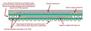
Side-view schematic of a typical flip chip mounting

Processing a flip chip is similar to conventional IC fabrication, with a few additional steps.[1] Near the end of the manufacturing process, the attachment pads are metalized to make them more receptive to solder. This typically consists of several treatments. A small dot of solder is then deposited on each metalized pad. The chips are then cut out of the wafer as normal.

Recently, high-speed mounting methods evolved through a cooperation between Reel Service Ltd. and Siemens AG in the development of a high speed mounting tape known as ‘MicroTape.'[1]. By adding a tape-and-reel process into the assembly methodology, placement at high speed, typically 20,000 placements per hour are achievable using standard PCB assembly equipment.[citation needed]

To attach the flip chip into a circuit, the chip is inverted to bring the solder dots down onto connectors on the underlying electronics or circuit board. The solder is then re-melted to produce an electrical connection, typically using an ultrasonic or alternatively reflow solder process. This also leaves a small space between the chip’s circuitry and the underlying mounting. In most cases an electrically-insulating adhesive is then “underfilled” to provide a stronger mechanical connection, provide a heat bridge, and to ensure the solder joints are not stressed due to differential heating of the chip and the rest of the system.

Advantages

The resulting completed flip chip assembly is much smaller than a traditional carrier-based system; the chip sits directly on the circuit board, and is much smaller than the carrier both in area and height. The short wires greatly reduce inductance, allowing higher-speed signals, and also conduct heat better.

Disadvantages

Flip chips have several disadvantages. The lack of a carrier means they are not suitable for easy replacement, or manual installation. They also require very flat surfaces to mount to, which is not always easy to arrange, or sometimes difficult to maintain as the boards heat and cool. Also, the short connections are very stiff, so the thermal expansion of the chip must be matched to the supporting board or the connections can crack.[2] The underfill material acts as an intermediate between the difference in CTE of the chip and board.

History

The process was originally introduced commercially by IBM in the 1960s for individual transistors and diodes packaged for use in their mainframe systems.[3] DEC followed IBM’s lead, but was unable to achieve the quality they demanded, and eventually gave up on the concept. It was pursued once again in the mid-90s for the Alpha product line, but then abandoned due to the fragmentation of the company and subsequent sale to Compaq. In the 1970s it was taken up by Delco Electronics, and has since become very common in automotive applications.

Alternatives

Since the flip chip’s introduction a number of alternatives to the solder bumps have been introduced, including goldballs or molded studs, electrically conductive polymer and the “plated bump” process that removes an insulating plating by chemical means. Flip chips have recently gained popularity among manufacturers of cell phones, pagers and other small electronics where the size savings are valuable.[citation needed]

See also

  • Solid Logic Technology
  • IBM 3081

References

  1. ^ Solder Bump Flip Chip
  2. ^ Demerjian, Charlie (2008-12-17), Nvidia chips show underfill problems, The Inquirer, retrieved 2009-01-30
  3. ^ Introduction to Flip Chip: What, Why, How

Further reading

  • Wikihowto: Guide to IC packages
0

再谈硬度的分类

之前在《关于硬度的等级和单位》一文中大概探讨了邵氏硬度A、D、00等的区别,不过从一个卖硬度计的网站上找到了更全面的分类,摘抄如下。其中一个疑问就是之前我所理解的邵氏硬度就是Shore,而该文中这个称谓肖氏硬度,而我之前一直以为邵氏硬度和肖氏硬度是同一个单位,只是将Shore不同的音译方式而已。

硬度表示材料抵抗硬物体压入其表面的能力。它是金属材料的重要性能指标之一。一般硬度越高,耐磨性越好。常用的硬度指标有里氏硬度计,洛氏硬度计,布氏硬度计,维氏硬度计

显微硬度计(从维氏硬度计里独立分类),肖氏硬度计,邵氏硬度计,巴氏硬度计,铅笔硬度计

1.里氏硬度计。这是一种能将各种硬度值进行换算的较小型的硬度计。主要用于对金属材料的测试,特别是对较大型的工件。由于有多种冲击装置,购买时要根据具体需要来选定。主要是用于模具的测试,因一般的洛氏硬度计很难对大型的模具进行测试。我国还未有这方面的国家标准,用里氏硬度计测试后的数据可进行转换。

2. 洛氏硬度计。用于各种钢材(含合金钢、不锈钢)硬度的测试。这是最重要的、最常用的一类硬度计。有以下几种:

①洛氏硬度计。指手动打硬度的,指针显示的。这是最早也是最普通用于钢材硬度测试的硬度计,可以测硬质合金、淬火钢和未经淬火钢材。硬度较软的铸铁、薄于2毫米的板材均不适合于用此种硬度计。

有三种试验力,从小到大,共有三种硬度:HRA、HRB、HRC,其中淬火钢材、模具钢常用HRC。

② 电动洛氏硬度计。性能同①。不用人工手动打硬度,可以得到较准确的数据。

③ 数显洛氏硬度计。性能同②。其为数字显示,读数方便。

④ 数显表面洛氏硬度计。当金属硬度层比较薄时,如用一般洛氏硬度计就会将硬度层打穿,而测不到其表面硬度层的真正硬度。这时要用洛氏表面硬度计。由于表面层较薄,人工手动打就不易控制,一般都为电动,且为数显,所以是数显表面洛氏硬度计。用于经过渗碳或渗氮的钢材、电镀层为主,以及用于想知道金属如钢材、合金钢、硬质合金表面的硬度。

⑤ 数显洛氏、表面洛氏硬度计。能测一般的洛氏硬度,又能测表面洛氏硬度。根据压头匹配和标尺选择,可测参数为HRA、B、C、D、E、F、G、H和K。CPU数据处理。机子除配有打印机外,还有RS-232计算机接口。

3.布氏硬度计。测未经淬火的钢材、铸铁、有色金属及质软的轴承合金材料,用HBW表示。除一般数显布氏硬度计外,还有携带式布氏硬度计、锤击式布氏硬度计和门式布氏硬度计。布氏硬度(HB)一般用于材料较软的时候,如有色金属、热处理之前或退火后的钢铁。洛氏硬度(HRC)一般用于硬度较高的材料,如热处理后的硬度等等。布式硬度(HB)是以一定大小的试验载荷,将一定直径的淬硬钢球或硬质合金球压入被测金属表面,保持规定时间,然后卸荷,测量被测表面压痕直径。布式硬度值是载荷除以压痕球形表面积所得的商。一般为:以一定的载荷(一般3000kg)把一定大小(直径一般为10mm)的淬硬钢球压入材料表面,保持一段时间,去载后,负荷与其压痕面积之比值,即为布氏硬度值(HB),单位为公斤力/mm2 (N/mm2)。

4.维氏硬度计。用于测黑色金属、有色金属、硬质合金(如铝合金)及表面渗碳、渗氮层的硬度,用HV表示。 对于表面层很薄、硬度又较低的材料,要用小负荷维氏硬度计。这种硬度计带有显微镜(有的生产厂称为显微硬度计)以便观察打出的凹痕,有的还配有编程计算器,能使硬度值的计算迅速准确。还有一种称微小维氏硬度计,最小试验力只有10克力(10gf)。

5.邵氏硬度计为橡胶A型硬度计,是一种手持式硬度计,可精确橡胶(塑料)制品的邵氏硬度,它测量了规定压针在指定压强和时间条件下的针入度,是现场使用理想的测试仪器。它具有携带方便、造型美观、重量轻等优点。

6.肖氏硬度 – Shore scleroscope hardness

说明:简称HS。表示材料硬度的一种标准。由英国人肖尔(Albert F.Shore)首先提出。应用弹性回跳法将撞销从一定高度落到所试材料的表面上而发生回跳。撞销是一只具有尖端的小锥,尖端上常镶有金刚钻。用测得的撞销回跳的高度来表示硬度。肖氏硬度计适用于测定黑色金属和有色金属的肖氏硬度值。用于测定橡胶、塑料、金属材料等的硬度。在橡胶、塑料行业中常称作邵氏硬度。

7.巴柯尔(Barcol)硬度(简称巴氏硬度), 最早由美国 Barber-Colman公司提出,是近代国际上广泛采用的一种硬度门类,以特定压头在标准弹簧的压力作用下压入试样,以压痕的深浅表征试样的硬度。巴柯尔硬度计(巴氏硬度计)作为专门测量玻璃钢制品、增强或非增强硬塑料、铝及铝合金、黄铜、紫铜等较软金属硬度的专用检测工具(特别 适用于玻璃钢制品),已被大多数国家或国际组织认可。美国材料试验协会(ASTM)、日本工业规范(JIS)、中国等国家相继制定《用巴柯尔硬度计测量玻璃钢(GRP)硬度试验方法》的国家标准。

    联系站长

    • Name:QiuBo QQ:1808976
      Email:Anndiqiu#Gmail.com
      Mobile Phone:13923499497

    热门文章

    添加站长微信,与站长在线实时交流

    QQ不在线时请用微信

链接